Introduction

Introduction to the world of the smallest parts

Nano is a prefix that marks the billionth part of something (10-9), comes from the Greek and literally means dwarf. So it's actually something very small, not just invisible to the eyes, but also not visible with conventional microscopes. Technology means the application of knowledge in technical processes, ie for the production of products. So what can be so special about something you almost can not perceive and how can you make products for which extreme growth rates are predicted in the future?

The development of nanotechnology (NT) was accelerated and by the development of scanning tunneling or scanning probe microscopy developed by IBM in the mid-80s of the last century. This makes it possible not only to make individual atoms "visible" but also to manipulate them with specially equipped finest tips.

Nanotechnology is the application of nanosciences - the study of nanoscaled systems - which can be the basis for future products and processes. These include, for example, many biological systems that are  nanoscale in their functional units (eg, DNA), forming the basis of life.
Size-dependent properties of nanomaterials

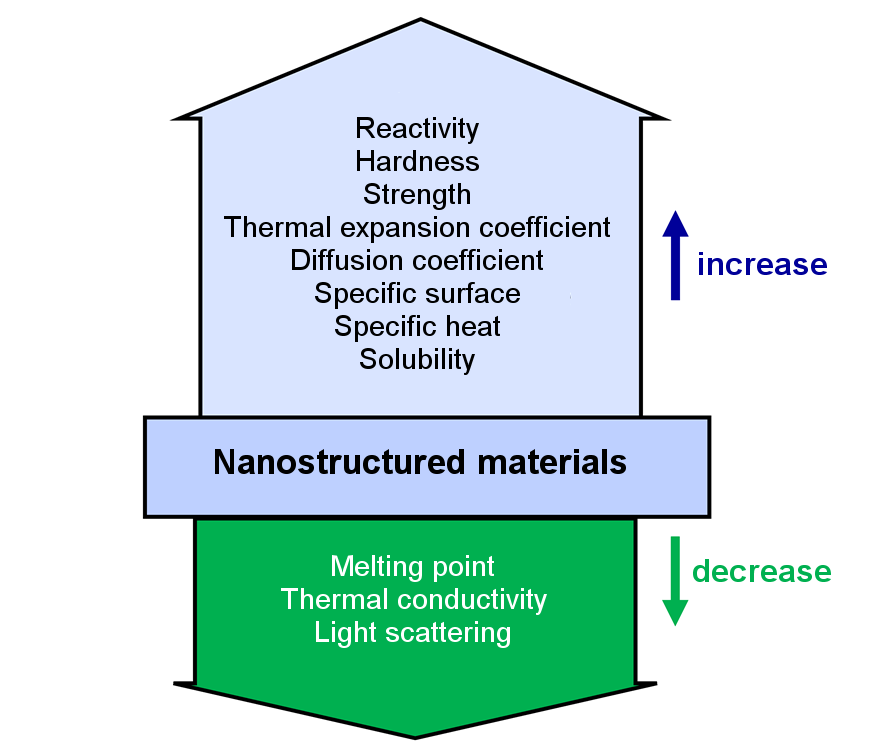
Overview: Size-dependent properties of nanomaterials.
© Fraunhofer ISC
Overview: Size-dependent properties of nanomaterials.

An important reason why NT seems so interesting for technical developments is that properties of materials in the nano-range depend on their size and shape (particle, fiber, platelets) - a behavior that is not known from the macroscopic world. For material developers, this offers very interesting possibilities, since in addition to the molecular structure and the composition, the size / shape of the subunits is also available as an additional parameter for the control of desired properties.

Do special laws govern the nano world? No, all physical and chemical laws are in place. They are only applied to units that are located between atomic / molecular and macroscopic systems. Nanoscale systems are therefore often referred to as mesoscopic.

Increased influence of surface atoms

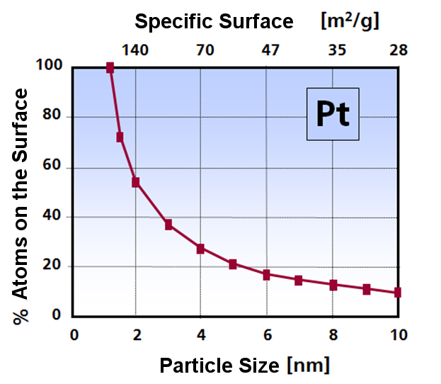
Atoms on the surface of a Pt particle as a function of particle size and increase in specific surface area.
© Fraunhofer ISC
Atoms on the surface of a Pt particle as a function of particle size and increase in specific surface area.

The number of atoms of a material, which are at its surface, increases very strongly with decreasing particle sizes. Thus, in the extreme case of a 2 nm platinum particle, more than 50 percent of all atoms can be found at the surface / interface and the specific surface area of the particle increases sharply. Also in bulk materials with nanoscale grains such as nanoscale ceramics or metals especially the mechanical properties are determined significantly by the grain sizes.

Since surface atoms have fewer neighbors than those inside the material, they have higher energy and are more reactive. This results in lowering of the melting point, thermodynamically stable intermediate phases or especially by an increased catalytic activity of materials.

Confinement: Change of optical and electrical properties

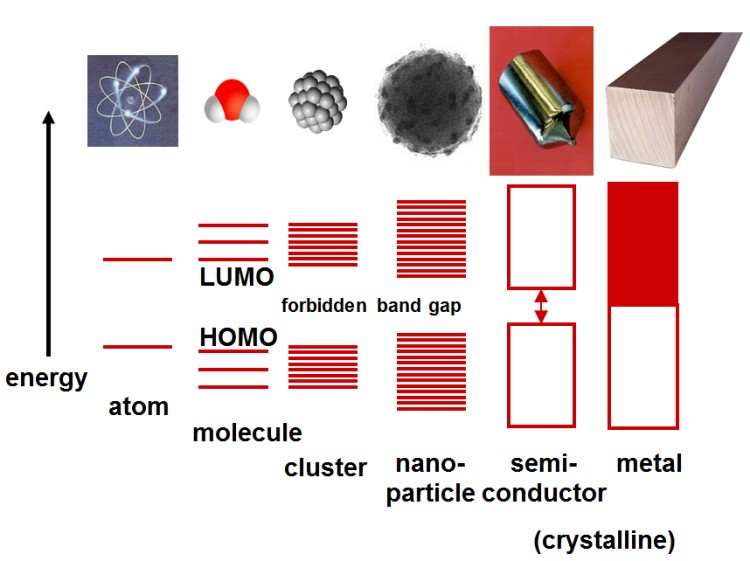
Dependence of the band structure of semiconductors and metals as a function of size.
© Fraunhofer-ISC
Dependence of the band structure of semiconductors and metals as a function of size.
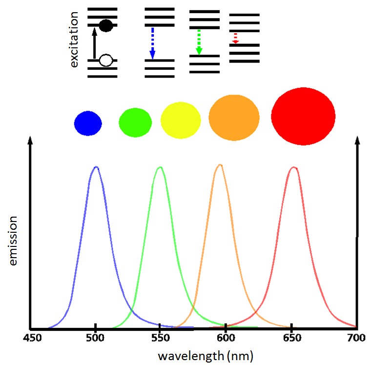
Example of size dependent optical properties of quantum dots (semiconductor nanoparticles): fluorescence emission.
© S. Logothetidis (2012)
Example of size dependent optical properties of quantum dots (semiconductor nanoparticles): fluorescence emission.

The electronic and optical properties of metals and semiconductors also depend very much on the system size (picture left). For example, discrete molecular orbitals with defined LUMO (lowest unoccupied molecular orbital) and HOMO (highest occupied molecular orbital) states dominate in molecules. With increasing size e.g. in clusters the energy states change e.g. the band gap is lowering. A further increase in the system size leads to the known energy states of semiconductors or metals. In the nanoscale intermediate region between atomic and macroscopic states, optical properties can therefore be changed in a controlled manner. This results in the change of absorption (color) or fluorescence of semiconductor particles (quantum dots). The confinement, ie the limitation of the charge carrier movement in nanostructures, as in thin films, wires or in all three spatial directions of nanoparticles, is the basis for many applications of nanoscale systems in optics (lasers, biosensors, etc.).